LEAPER Visual Inspection Solutions for Semiconductors
Home / Applications / Semiconductor

Leaper WaferScan Toolkit

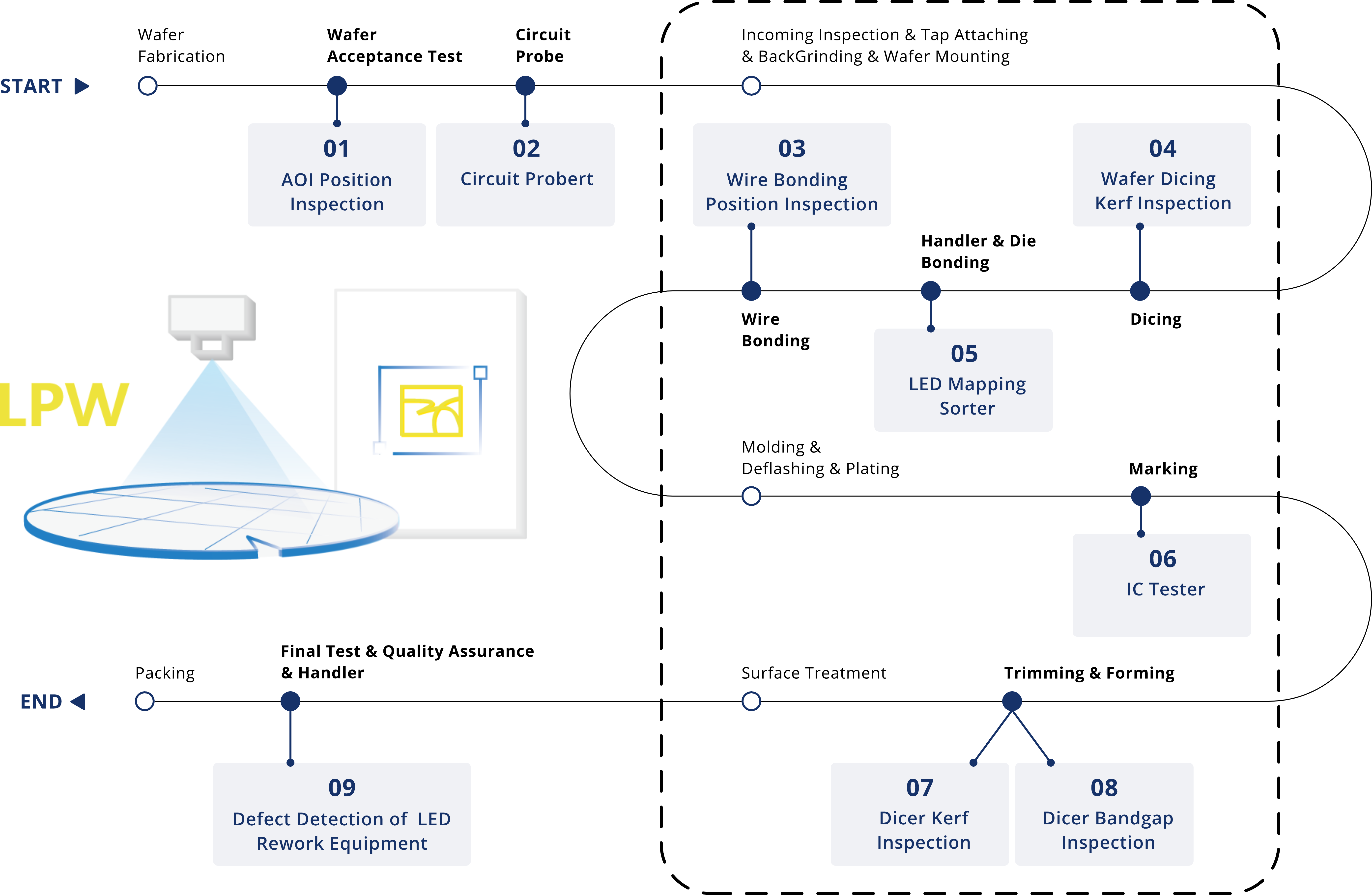
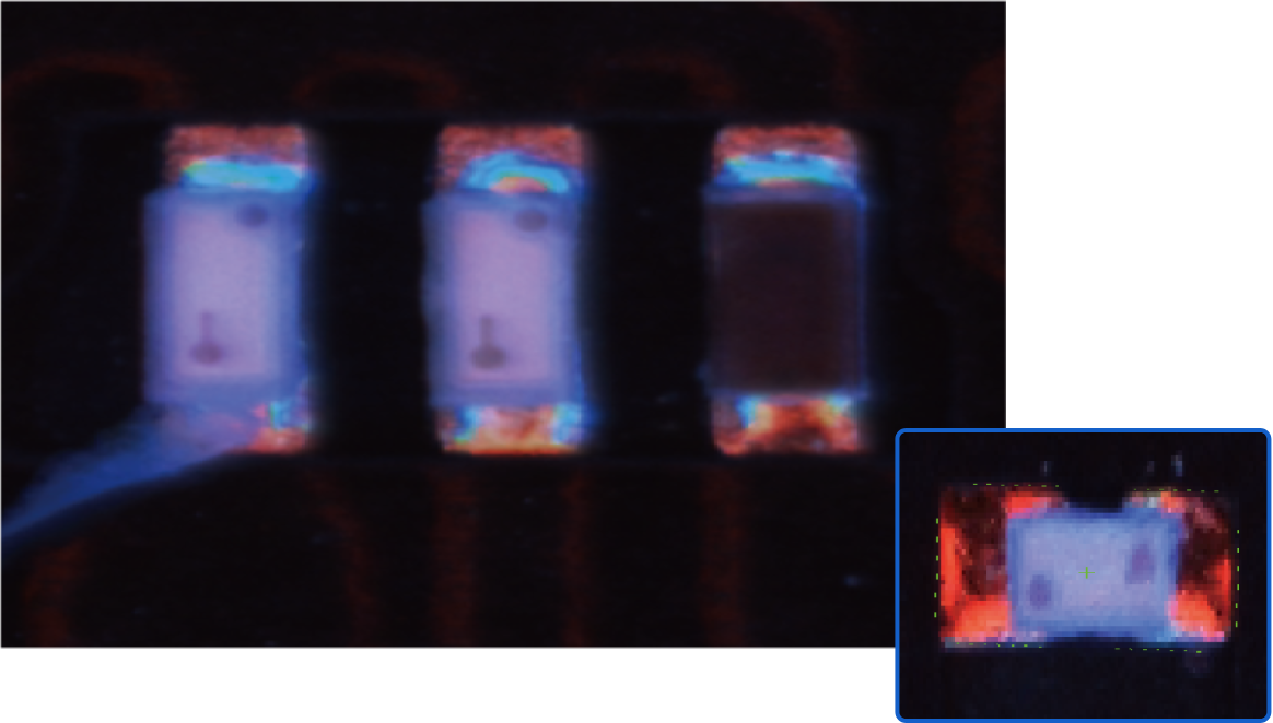
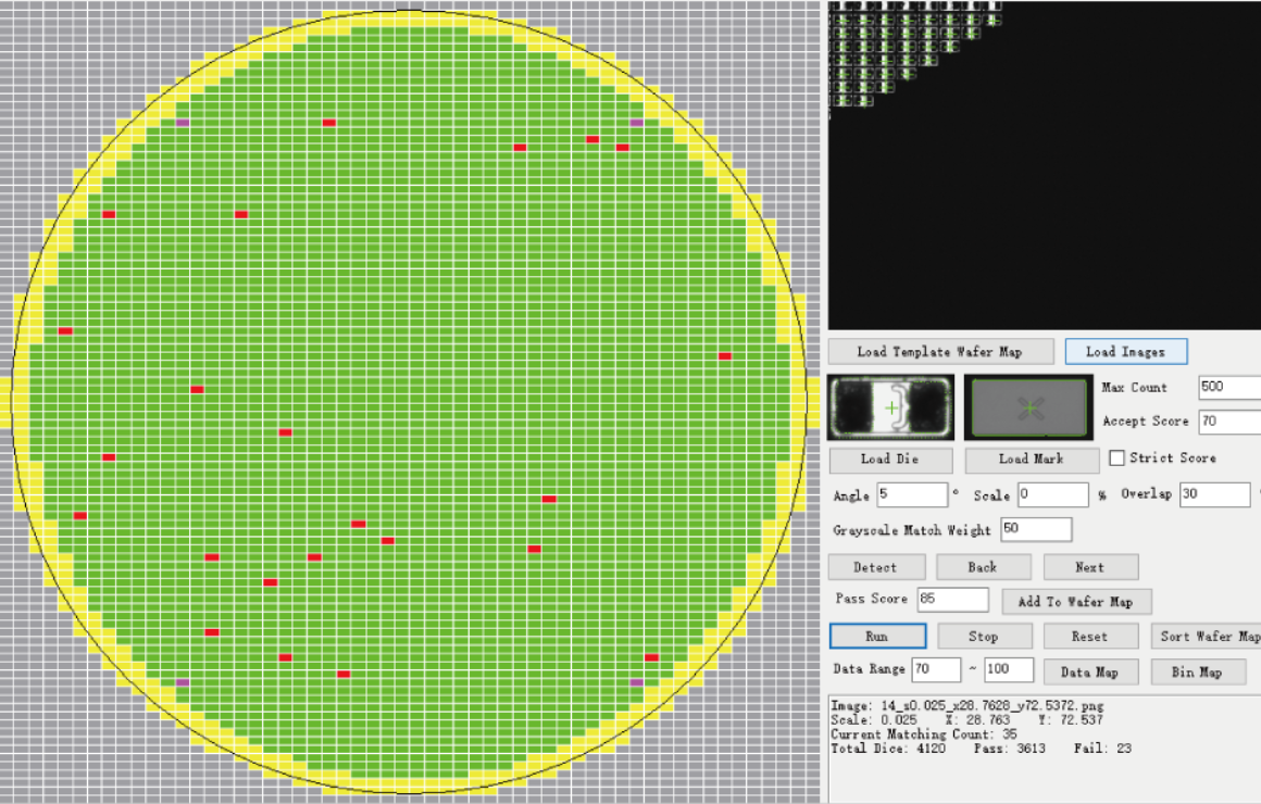
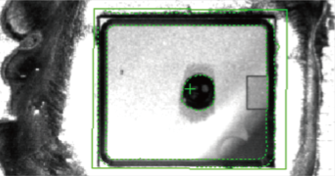
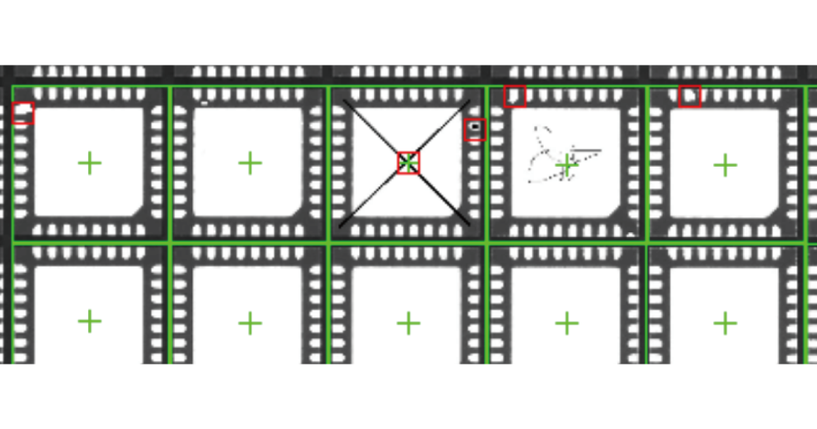
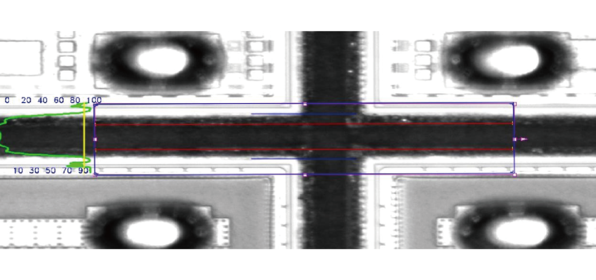
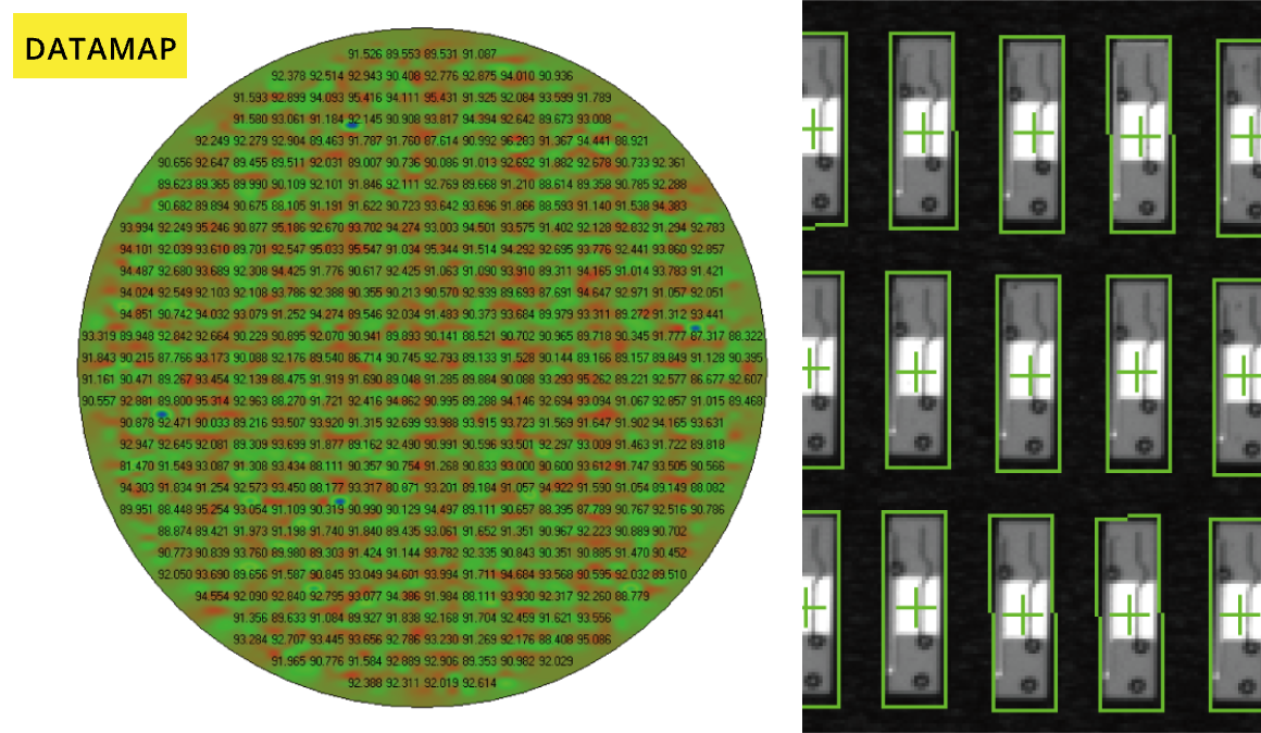
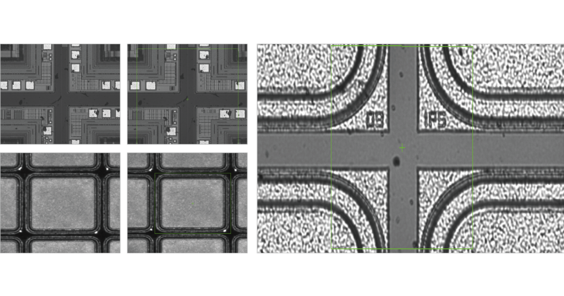
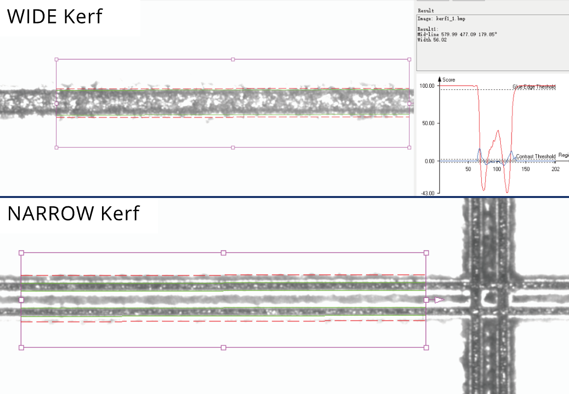
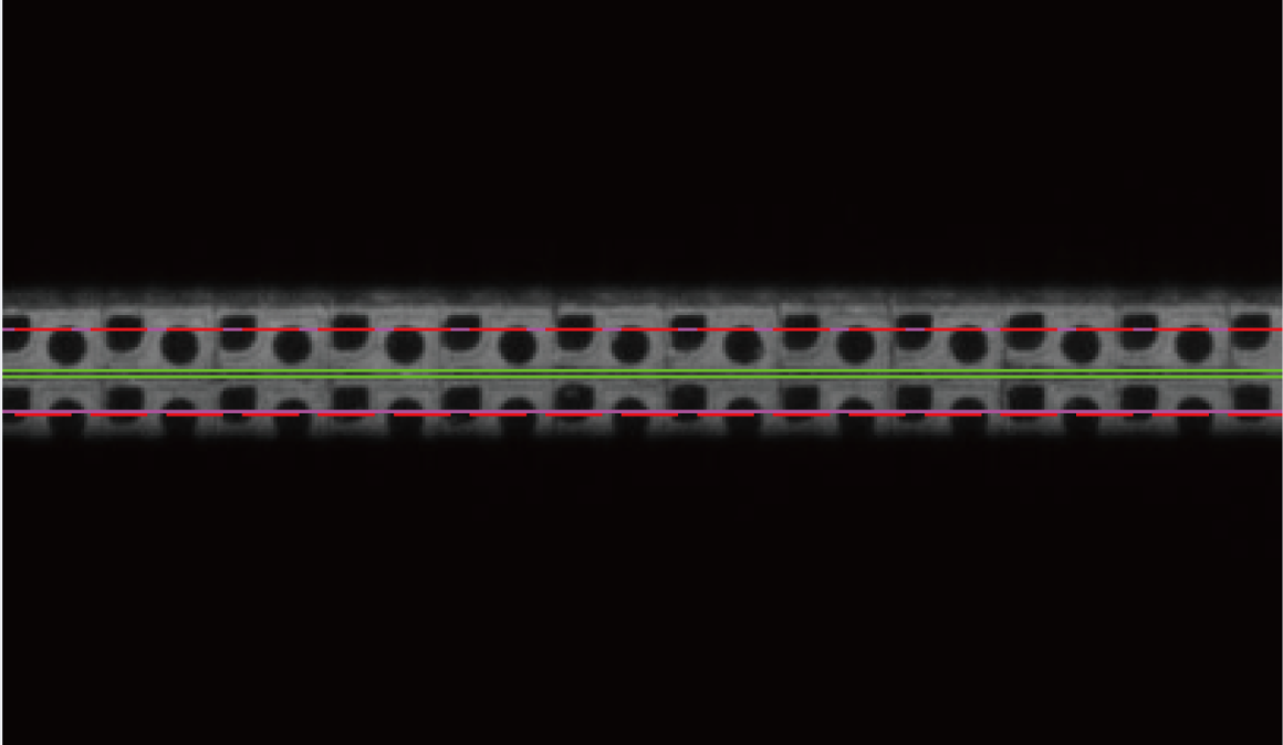
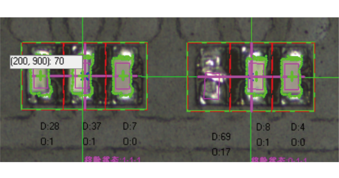
Leaper WaferScan Toolkit (LPW) is designed to help user build the widest range of machine vision applications with ultimate flexibility. LPW allows developers to write their own vision processing, configure multi-threading, and access all tool properties and options. Cost-effective, high-quality production of semiconductors and LEDs require speed, accuracy and frictionless tracking through the whole fabrication. Semiconductor manufacturers and OEMs rely on LEAPER machine vision technology to ensure precise alignment of wafers during sorting, counting, masking and etching processes, increase traceability of wafers and die as they move through the front and back-end processes, and improve product quality through advanced inspection procedures.
Leaper WaferScan Toolkit Visual Inspection Process


AOI Position Inspection
  • IInspection Requirements: Identification and positioning of LED components.
  • Detection Accuracy: XY offset ≤ ± 40μm, angular deflection ≤ ± 9°
  • Detection Speed: 60s /90,000 PCS
  • Detection Solution: Realize the positioning of bounding pads and chips through template matching and image processing.

Circuit Probert
  • Inspection Requirements: Positioning of LED chips, forming a map of the wafer, and marking.
  • Detection Accuracy: < 0.2 pixels
  • Detection Speed: 70ms / 400 PCS / 6MP, 180ms / 4500 PCS / 1.5MP
  • Detection Solution: Realize high-speed and accurate die positioning during wafer scanning, and remove twins and bad dies based on die arrangement, as well as generate waferMap in real time according to die coordinates and data.

Wire Bonding Position Inspection
  • Inspection Requirements: Accurately locate the pad to achieve wire bonding between the lead and pad.
  • Detection Accuracy: 2pixels
  • Detection Speed: 8ms
  • Detection Solution: Template matching based on shape and machine learning to realize pad positioning in environments with uneven pad imaging quality and large background interference.

Wafer Dicing Kerf Inspection
(1) Wafer Sawing
  • Detection Accuracy: 0.5pixels
  • Detection Speed: 120ms
  • Inspection Solution: template matching algorithm to locate the packaged chip, Kerf algorithm to detect the position and width of the dicing line, geometric algorithm to detect the size of the lead and pad of the packaged chip, and AOI algorithm to locate the defects of the lead and pad.

Wafer Dicing Kerf Inspection
(2) Laser Dicer
  • Detection Accuracy: 1μm
  • Detection Speed: 20ms
  • Detection Solution: Kerf algorithm realizes the center position positioning of the dicing line and the measurement of the dicing line size. Double edge detection can be used in the scene with large interference.

LED Mapping Sorter
  • Inspection Requirements: Accurately provide chip positions, detect and eliminate chip defects, such as twins, notch, dirt, large angle deviations, etc.
  • Detection Accuracy: 0.3pixels, angle < 1°
  • Detection Speed: 100-300ms
  • Detection Solution: Use template matching to locate the chips in the wafer, image preprocessing and Blob to filter abnormal chip data, then sort the remains and provide them to the equipment pick up.

IC Tester
  • Inspection Requirements: For the precise positioning of chips in complex backgrounds.
  • Detection Accuracy: 0.3pixels
  • Detection Speed: 30ms
  • Detection Solution: Template matching realizes the positioning of the IC chip, the gauge realizes the wafer edge inspection, and the blob realizes the needle mark detection.

Dicer Kerf Inspection
  • Inspection Requirements: Wafer cutting line position, size and chipping inspection.
  • Detection Accuracy: 1μm
  • Detection Speed: 20ms
  • Detection Solution: Kerf algorithm realizes the positioning and measurement of the cutting line. Double-edge detection scheme can be used in scenes with large interference.

Dicer Bandgap Inspection
  • Inspection Requirement: Dicing line inspection for Mini LED chips, and also used for most conventional LED chips.
  • Detection Accuracy: 0.5pixels
  • Detection Speed: 40ms
  • Detection Solution: Kerf algorithm realizes crack gap detection before and after the dicing, judges whether the wafer is completely fractured, and then adjusts the cutting depth.

Defect Detection of LED Rework Equipment
  • Inspection Requirements: Identify and position pads and chips.
  • Detection Accuracy: 2pixels
  • Detection Speed: 300ms
  • Detection Solution: Image preprocessing, template matching and array sorting to realize pad positioning, search for internal LED die position and quality based on pad position.