Vision-Based Inspection Solution for Photovoltaic
Home / Applications / Photovoltaic / Micro Crack

Micro Crack Inspection Module for Crystalline Silicon Cells

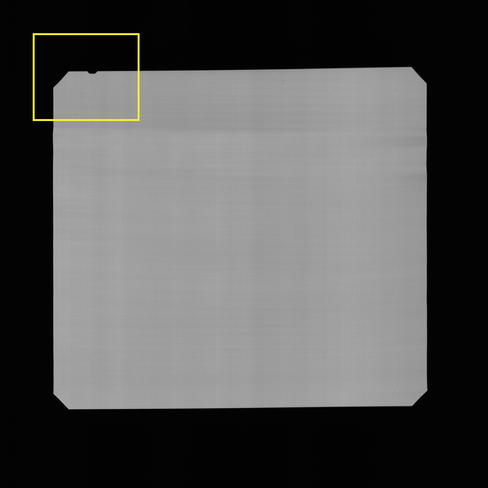
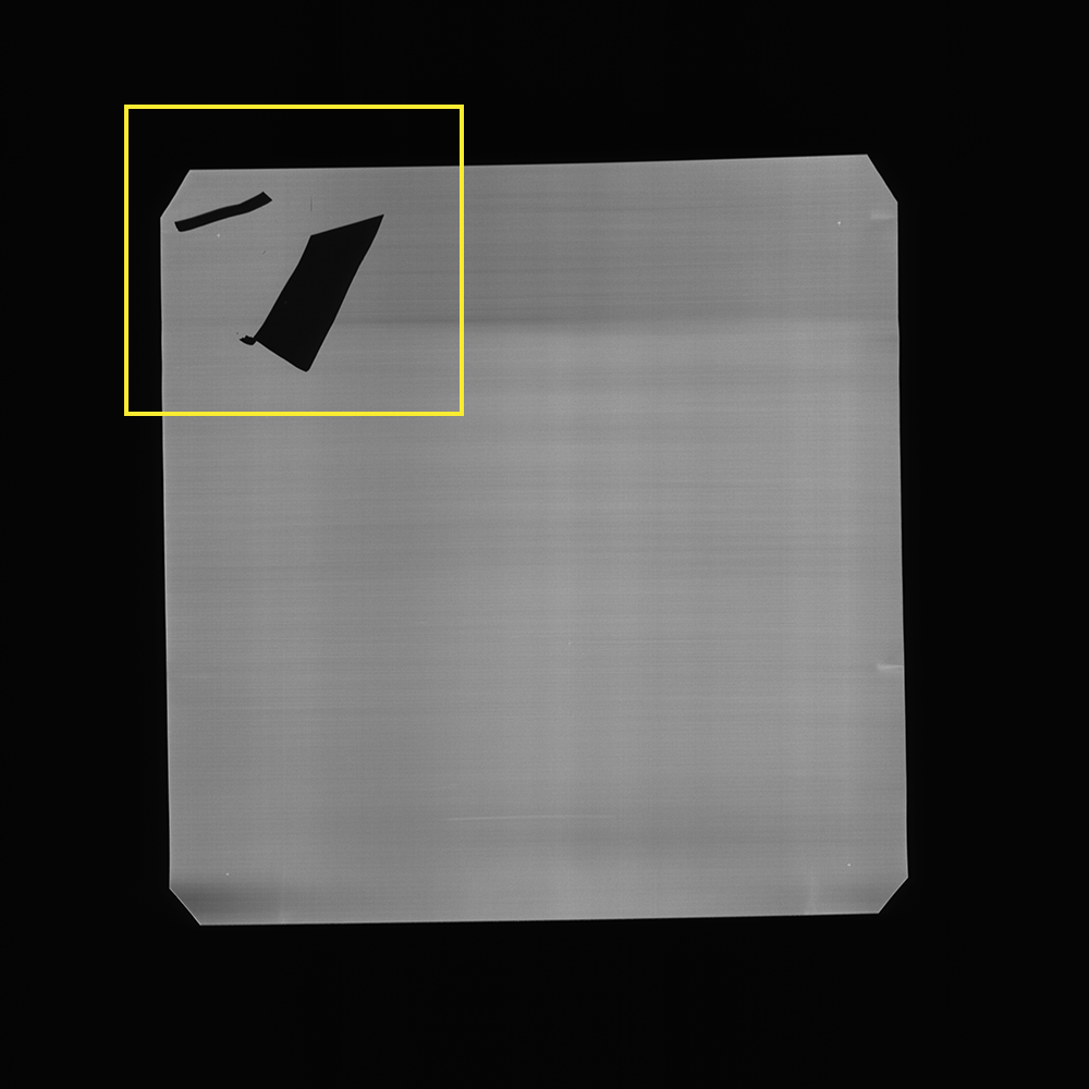
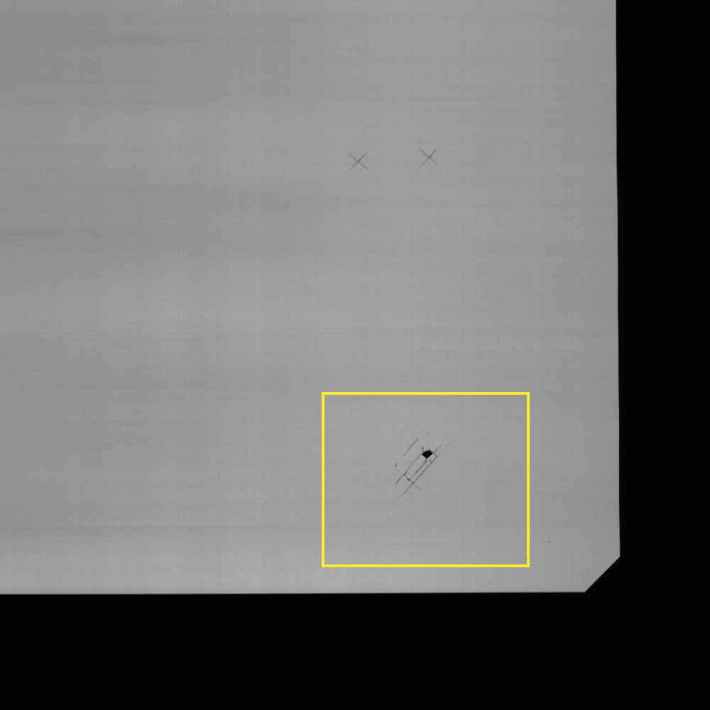
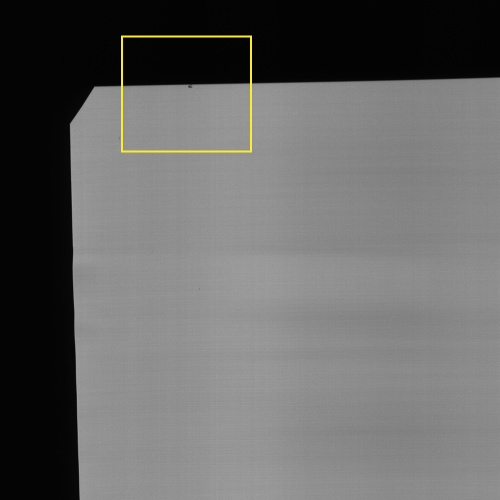
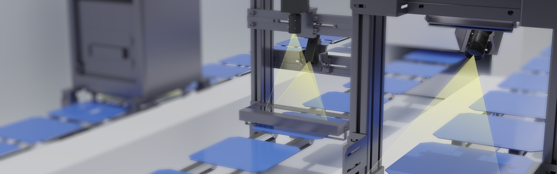
Mainly used for the inspection of defects such as micro cracks in incoming silicon wafers.


Product Advantages

· Inspection module of integrated micro crack fragment

· Fully customized optical system (sold at a lower price with a better performance)

· High-efficient AI algorithm (with an algorithm time of 100ms or less)


Defect Images
SC-A100
SC-B300
SC-C300
  • Capacity
    Single track ≤ 4500 Pcs/H
  • Maximum Inspection Accuracy
    85 μm
  • Equipment Availability
    ≥ 99.5%
  • Breakage Rate
    < 0.05% (transmission rejection)
  • Repeatability
    99%
  • Voltage
    220V AV
  • Power
    ≤ 1.3KW
  • Solar Cells Type
    Applicable to cell size: 182mm~230mm, wafer thickness 110~220μm
  • Miss Inspection Rate of Normal Wafers
    ≤0.1%, calculation method: number of missed inspections/total number of detected wafers
  • Wrong Inspection Rate of Normal Wafers
    ≤0.1%, calculation method: number of false inspections/total number of inspections
  • Miss Inspection Rate of Reworked Wafers
    ≤2%, calculation method: number of missed inspection/total inspection wafers
  • Wrong Inspection Rate of Reworked Wafers
    ≤2%, calculation method: number of false inspections/total inspections