Log In
|
Register
|
Log out
EN
CN
EN
Home
Products
Leaper Vision Toolkit
IntelliBlink™
IntelliBlink-AI
Support
Software
Document
Company
About Us
Milestones
Global Deployment
Contact Us
Lead Scan
Semiconductors
Home
/
Applications
/
Semicon-Lead Scan
/
Bottom 2D/3D
Semicon-Lead Scan
Film
Planar Materials
Sheet Sorting Machine
RTS-AOI Sorter
RTP- Pre/Post-Offset Tester
Photovoltaic
Micro Crack
PECVD
PL
PE&PL
Cassette
Graphite Boat
Screen Printing
SE
Quartz boat inspection
Debris
Watermark
Final Product Sorting
Semiconductor
Semicon-DB AOI
Post-FC DB IR Inspection System
High-Speed Die Micro-crack Inspection System
Die Micro-crack Inspection Module
Semicon-Lead Scan
Bottom 2D/3D
Top 2D
Top 3D
4 Sides
PIC
Tape & Reel
IR
AI
Li-ion Battery
Laser
Logistics
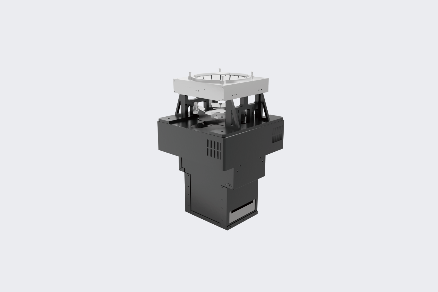
Bottom 2D/3D Vision Module
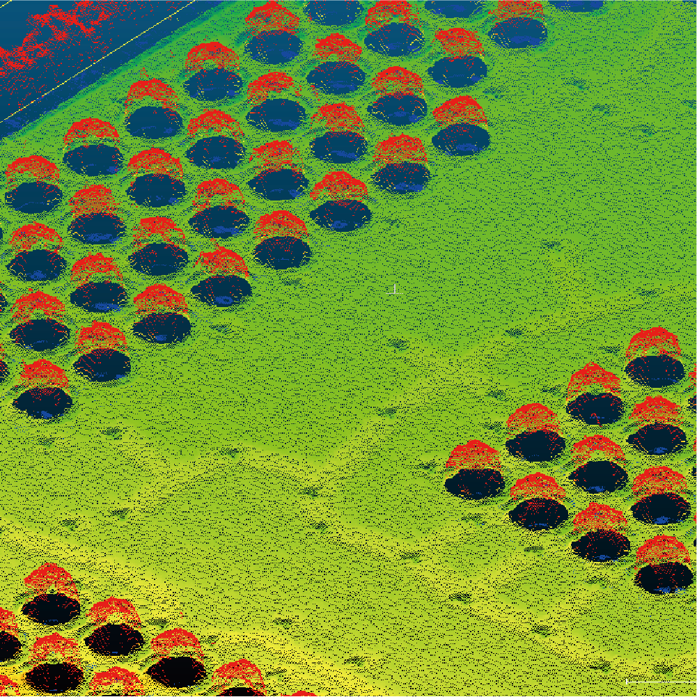
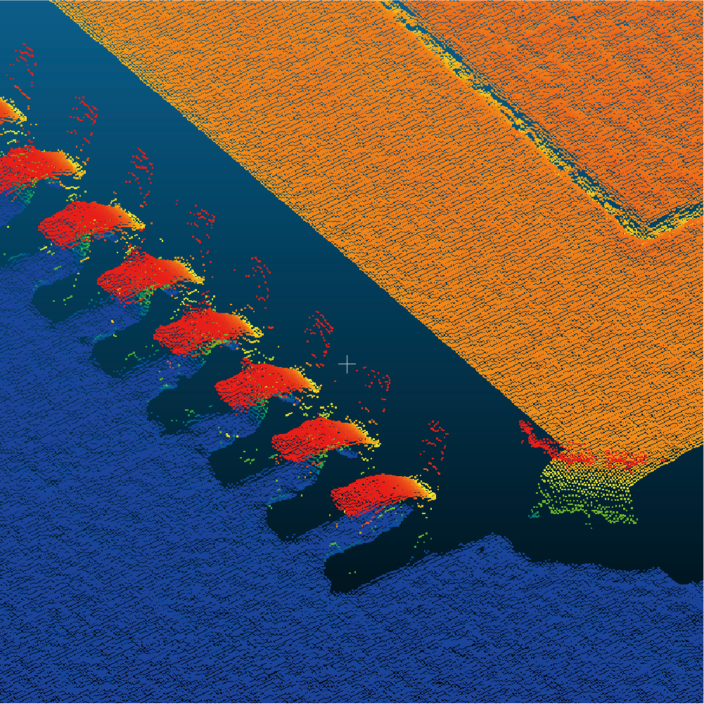
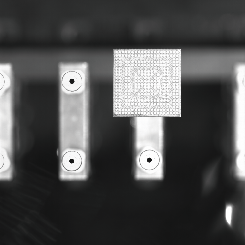
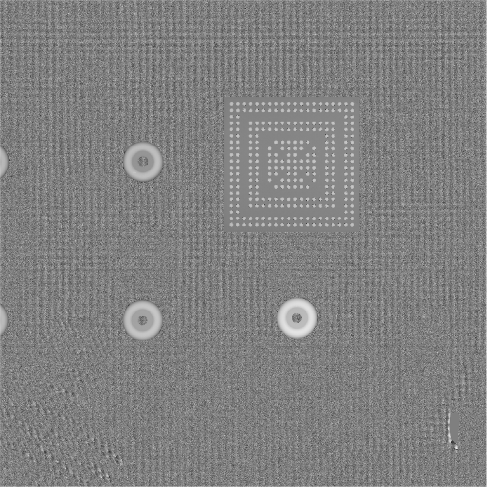
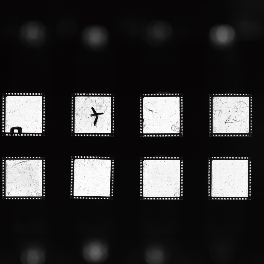
Performs bottom-side dimensional measurement and defect inspection of ICs, including but not limited to ball coplanarity, ball/pin/pad size, pin pitch, missing, extra, broken, or off-center balls, and passive component defects.
Defect Images
Technical Parameters
FOV
60mm × 60 mm ( 2.36in. × 2.36in.)
XY Lateral Resolution
12 μm
Pixels Per FOV
5120 × 5120
3D Sensor Height Resolution
< 0.2 μm
Repeatability
4 μm ( 3 σ )
Accuracy
± 3 μm
Minimum Feature Diameter
110 μm
Measurement Range
± 1 mm
3D Acquisition Time (Dwell), Typical
300 msec
Maximum Allowable Motion during Acquisition
3 μm
L × W × H
423.4mm × 423.4mm × 691mm
Weight
≈ 31 kg