Log In
|
Register
|
Log out
EN
CN
EN
Home
Products
Leaper Vision Toolkit
IntelliBlink™
IntelliBlink-AI
Support
Software
Document
Company
About Us
Milestones
Global Deployment
Contact Us
Lead Scan
Semiconductors
Home
/
Applications
/
Semicon-Lead Scan
/
Top 2D
Semicon-Lead Scan
Film
Planar Materials
Sheet Sorting Machine
RTS-AOI Sorter
RTP- Pre/Post-Offset Tester
Photovoltaic
Micro Crack
PECVD
PL
PE&PL
Cassette
Graphite Boat
Screen Printing
SE
Quartz boat inspection
Debris
Watermark
Final Product Sorting
Semiconductor
Semicon-DB AOI
Post-FC DB IR Inspection System
High-Speed Die Micro-crack Inspection System
Die Micro-crack Inspection Module
Semicon-Lead Scan
Bottom 2D/3D
Top 2D
Top 3D
4 Sides
PIC
Tape & Reel
IR
AI
Li-ion Battery
Laser
Logistics
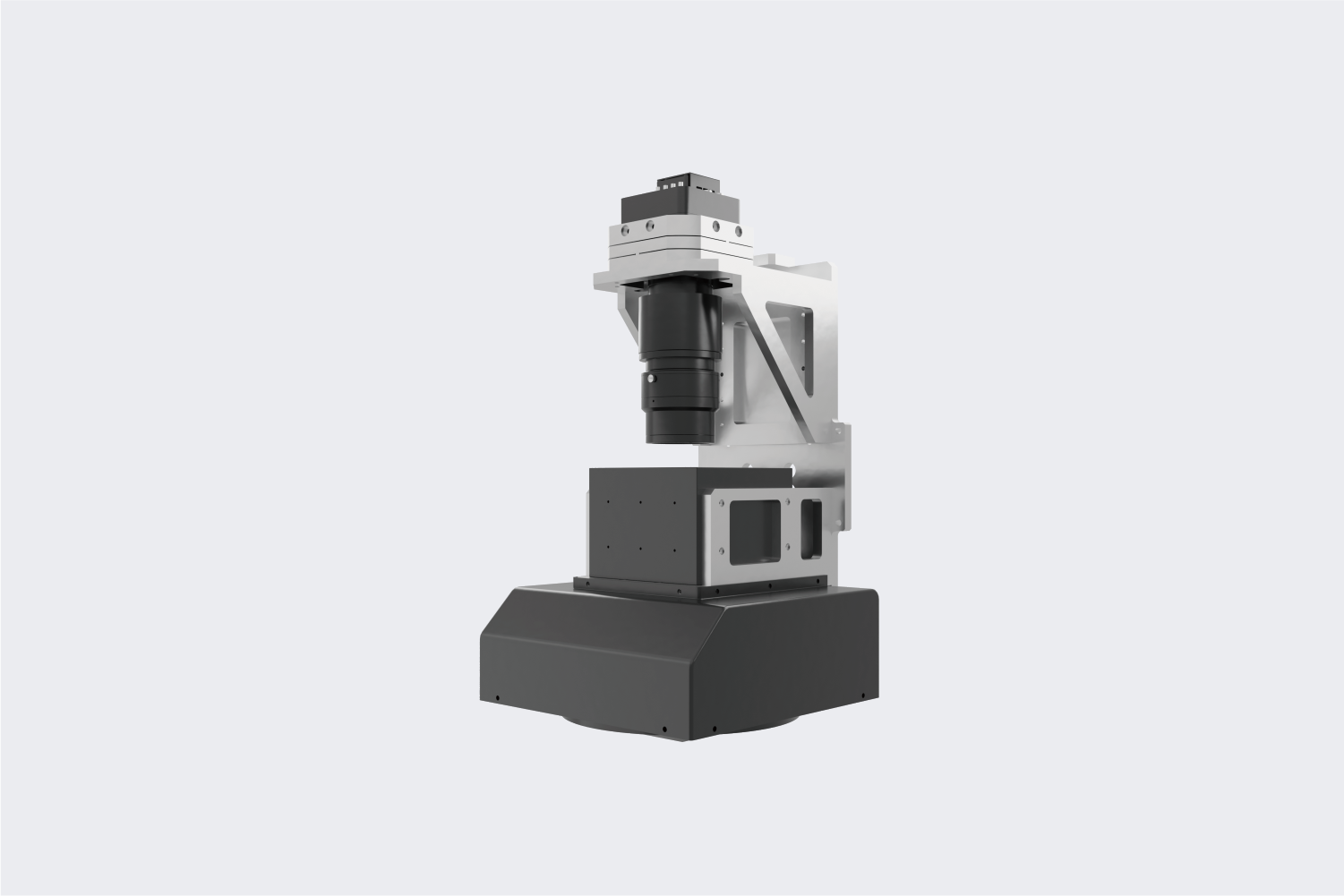
Top 2D Vision Module
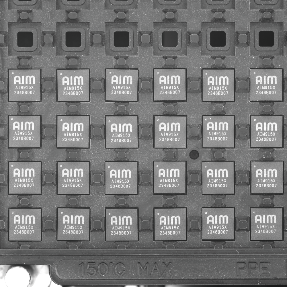
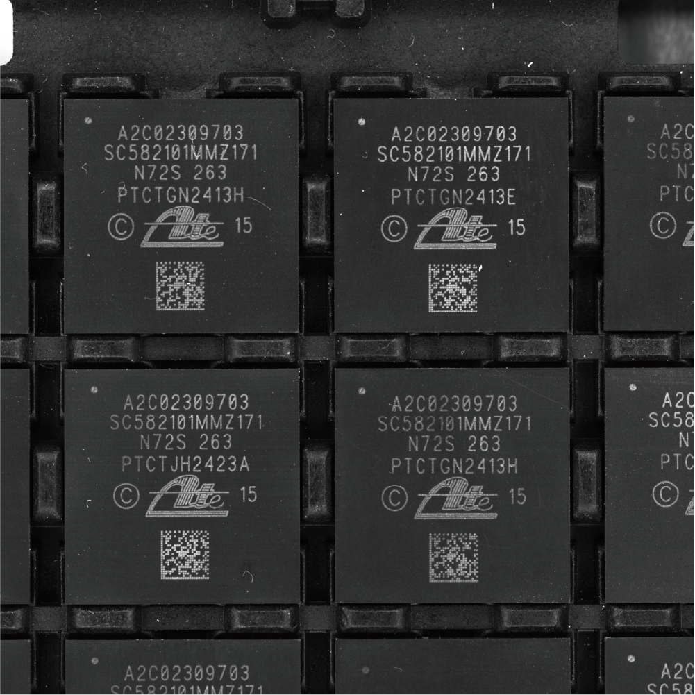
Performs top-side OCR recognition on IC products and detects surface defects, such as scratches, dents, dirt, and damage.
Defect Images
Technical Parameters
FOV
52mm × 52 mm
XY Lateral Resolution
10 μm
Pixels Per FOV
5120 × 5120
Min Defect
20 μm
Min Character Stroke Width
40 μm
Min Character Height
0.23 mm
Minimum grey value difference
30
L × W × H
254mm × 254mm × 462mm
Weight
≈ 15 kg